Upcoming prototype chip in TSMC 65nm Technology!
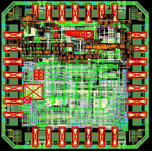
The prototype chip shown above has been fabricated in 65 nm UMC process. It consists of multiple transceiver architectures for chip-to-chip communications. Details of the transceiver can be found in Link1 and Link2.

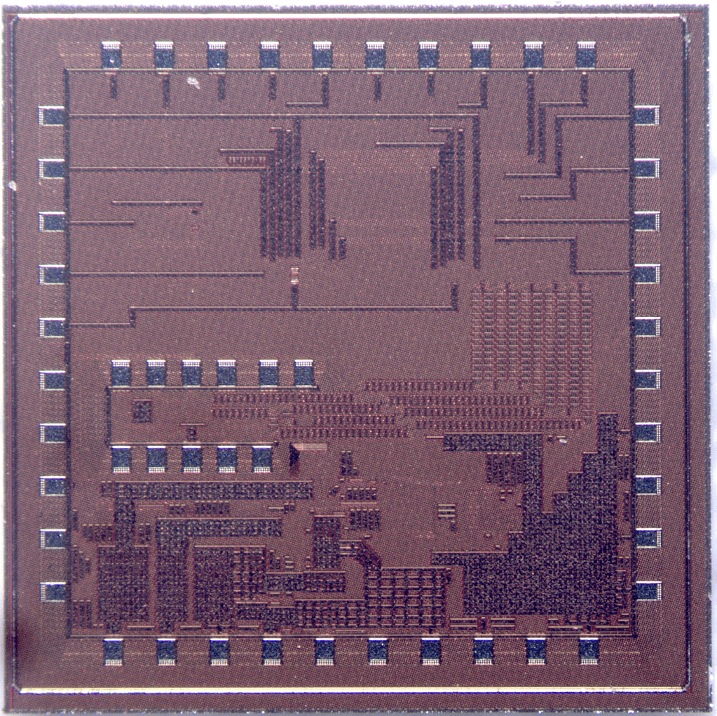
The test chip shown above has been fabricated in 180 nm UMC process. It consists of three different transceiver architectures of on-chip interconnect. The summary of the achievements of the test chip are:
- The current-mode differential coded transceiver achieved a speed of 9.25 Gb/s for a 5 mm long interconnect with an energy efficiency of 1.24 pJ/b. [Link]
- Full-duplex transceiver achieved a speed of 4.0 Gb/s for an energy efficiency of 0.95 pJ/b for 5 mm long interconnect. [Link]
- The transceiver for bus interconnect achieved a speed of 3.0 Gb/s for communication for an interconnect length of 4 mm.

The test chip shown above has been fabricated in 180 nm National Semiconductor process. It consists of low power current-mode receiver for on-chip interconnect. It was tested up to a data rate of 2.5 Gb/s for a global interconnect length of 10 mm. [Link]
